Photonic Neural Networks Accelerate Pattern Recognition in Industrial Quality Control Systems

Photonic neural networks combine optical components with neural network architectures to process visual data at speeds that exceed traditional electronic systems, and they target pattern recognition tasks in factories where rapid defect detection determines production line efficiency. Researchers integrate lasers, waveguides, and photodetectors on chips to perform matrix multiplications through light interference, which reduces the latency that electronic processors encounter when handling high-resolution images from assembly lines.
Industrial quality control systems rely on cameras and sensors to scan products for cracks, misalignments, or surface irregularities, yet conventional graphics processing units often struggle with throughput when multiple inspection stations operate simultaneously. Photonic implementations route photons through fixed or programmable interference patterns that directly encode learned weights, allowing classification decisions to emerge from optical measurements rather than sequential digital calculations.
Core Mechanisms Behind Photonic Acceleration
Light travels through silicon photonic circuits at speeds approaching the physical limit, and this property enables parallel computation across thousands of wavelengths within a single waveguide. Engineers encode input images as intensity or phase patterns at the input ports, while trained weights modulate the optical paths; the resulting interference pattern reaches detectors that output class probabilities without intermediate memory fetches. Data indicates that such architectures complete forward passes in picoseconds per inference when clocked by continuous-wave lasers, whereas electronic counterparts require nanoseconds or longer for equivalent operations.
Training occurs off-chip using conventional frameworks before weights transfer to the photonic hardware through thermo-optic or electro-optic phase shifters. Once configured, the network performs inference passively, consuming power mainly for laser sources and detector readout circuits. Observers note that energy per inference drops below one picojoule in optimized devices, a figure that supports always-on monitoring at conveyor speeds exceeding several meters per second.
Deployment Patterns in Manufacturing Environments
Automotive plants incorporate photonic accelerators into vision systems that inspect weld seams and paint finishes on moving vehicles. Cameras capture frames at rates above 1000 per second, and the optical neural network flags anomalies within microseconds, triggering mechanical diverters before defective parts advance further downstream. Similar setups appear in semiconductor fabs where photomask inspection demands sub-nanometer precision, and the low-latency classification prevents batches from proceeding with hidden contamination.
Textile and pharmaceutical lines adopt the same technology for surface texture analysis and pill imprint verification. Because photonic circuits tolerate high optical power without generating heat in the computation layer itself, facilities maintain stable temperatures around inspection stations, which protects both product integrity and measurement repeatability.
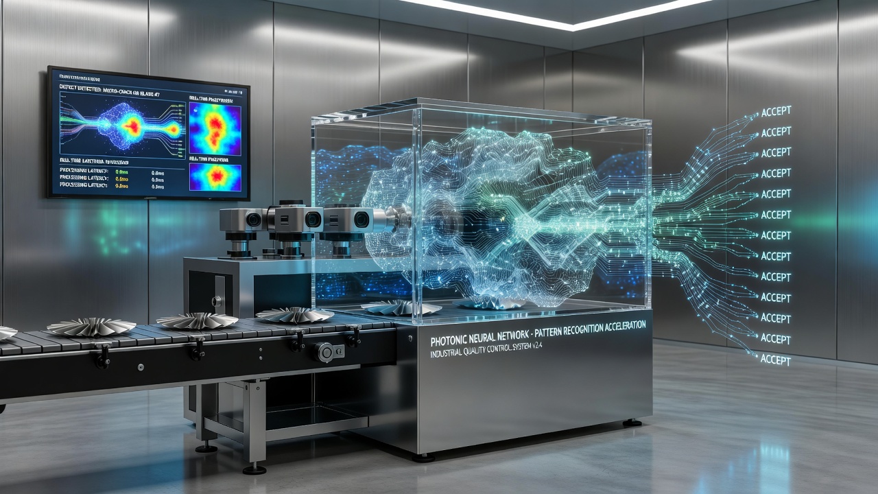
In July 2026, a collaborative project between European research institutes and North American equipment vendors demonstrated a photonic accelerator integrated directly into a bottling plant's inspection tunnel. The system processed 250,000 units per hour while maintaining false-positive rates below 0.02 percent, according to performance logs shared with participating manufacturers. The demonstration confirmed that wavelength-division multiplexing allowed simultaneous handling of visible and near-infrared inspection channels without additional electronic buffering.
Comparative Performance Metrics
Benchmarks published by academic laboratories show photonic networks achieving throughput improvements of 50 to 200 times over GPU baselines when restricted to fixed-pattern recognition workloads. Latency measurements drop from milliseconds to microseconds, enabling closed-loop control where rejected items are removed without halting the entire line. Accuracy remains comparable once training accounts for optical noise sources such as laser relative intensity noise and detector shot noise.
Cost analyses from industry reports indicate that initial photonic chip fabrication exceeds electronic alternatives, yet the reduction in downstream computing hardware and power infrastructure offsets the premium within two years of continuous operation. Maintenance requirements center on laser lifetime and fiber alignment stability rather than frequent firmware updates, which simplifies long-term deployment in harsh factory settings.
Integration Challenges and Current Solutions
Hybrid electro-optic interfaces still require analog-to-digital conversion at the detector outputs, and this step introduces a bottleneck that researchers mitigate through on-chip time-to-digital converters or analog decision circuits. Packaging photonic dies alongside electronic drivers demands sub-micron alignment tolerances, and foundries have responded by offering multi-project wafer runs that include standardized grating couplers for easier fiber attachment.
Calibration routines compensate for fabrication variations by periodically adjusting phase shifters with pilot optical signals. Those adjustments occur during scheduled maintenance windows, preserving uptime while keeping classification boundaries aligned with the original training distribution. Government-funded programs in Canada and Australia have supported open-source design kits that standardize these calibration sequences across different photonic foundry processes.
Future Scaling Directions
Three-dimensional stacking of photonic layers promises additional parallelism by routing light vertically through multiple planes of computation. Researchers explore materials such as lithium niobate on insulator and thin-film barium titanate to increase modulation bandwidth and reduce drive voltages. These advances support larger network depths without proportional increases in optical loss, which extends applicability to more complex inspection tasks such as multi-angle surface reconstruction.
Standardization efforts within international standards bodies focus on measurement protocols for optical neural network accuracy and power consumption, ensuring that performance claims remain comparable across vendors. Equipment suppliers have begun offering modular inspection heads that accept either electronic or photonic accelerator cards, allowing factories to upgrade incrementally as production volumes justify the transition.
Conclusion
Photonic neural networks deliver measurable gains in speed and energy efficiency for pattern recognition within industrial quality control pipelines, and ongoing hardware refinements continue to narrow remaining interface gaps. Manufacturing facilities that adopt these systems report sustained throughput improvements alongside reduced power draw at inspection points. Continued collaboration between photonic foundries, equipment integrators, and standards organizations supports broader deployment across sectors that depend on high-speed visual verification.